
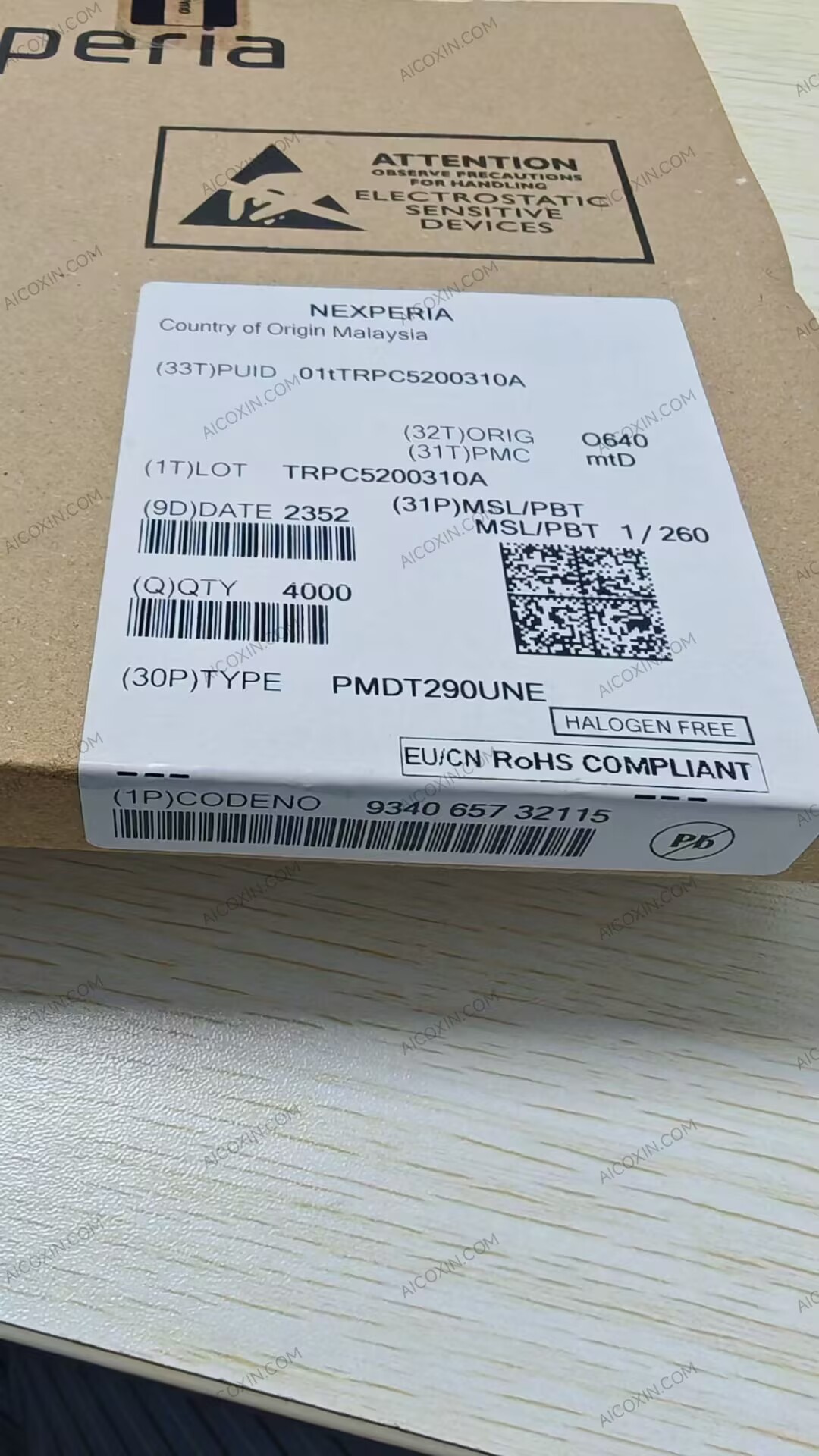

The Nexperia PMDT290UNE is a dual N-channel enhancement-mode Field-Effect Transistor featuring Trench MOSFET technology in an ultra-small SOT666 surface-mount package. Each transistor supports a 20V drain-source voltage and up to 800mA continuous drain current at VGS = 4.5V under the specified 25°C test conditions, making it suitable for compact low-voltage switching designs.
The PMDT290UNE is optimized for very fast switching and provides up to 2kV HBM ESD protection. Its drain-source ON resistance is typically 290mΩ and 380mΩ maximum at VGS = 4.5V and ID = 500mA. At VGS = 2.5V and ID = 400mA, maximum RDS(on) is 620mΩ.
Gate-source threshold voltage ranges from 0.5V to 0.95V, while peak drain current reaches 3.2A per transistor under the specified single-pulse conditions. Maximum total device power dissipation is 500mW on a standard PCB footprint, with a junction temperature range from -55°C to +150°C.
The device is housed in a 6-lead SOT666 package with 0.5mm pin pitch and a compact body measuring approximately 1.6 × 1.2 × 0.55mm. Typical applications identified by Nexperia include relay drivers, high-speed line drivers, low-side load switches, and general switching circuits.
Key Features:
- Manufacturer: Nexperia
- Part Number: PMDT290UNE
- Device Type: Dual MOSFET
- Configuration: Dual N-Channel
- Technology: Trench MOSFET
- Drain-Source Voltage: 20V
- Continuous Drain Current: 800mA per transistor
- Peak Drain Current: 3.2A
- Gate-Source Voltage: ±8V
- RDS(on): 290mΩ typ., 380mΩ max. at 4.5V
- RDS(on): 620mΩ max. at 2.5V
- Gate Threshold Voltage: 0.5V to 0.95V
- Total Gate Charge: 0.45nC typ.
- Input Capacitance: 55pF typ.
- ESD Protection: Up to 2kV HBM
- Maximum Device Power Dissipation: 500mW
- Junction Temperature: -55°C to +150°C
- Package: SOT666
- Pin Count: 6
- Pin Pitch: 0.5mm
- Package Size: Approx. 1.6 × 1.2 × 0.55mm
- Mounting Type: Surface Mount
- Applications: Relay drivers, high-speed line drivers, low-side load switches and switching circuits


Reviews
There are no reviews yet.