
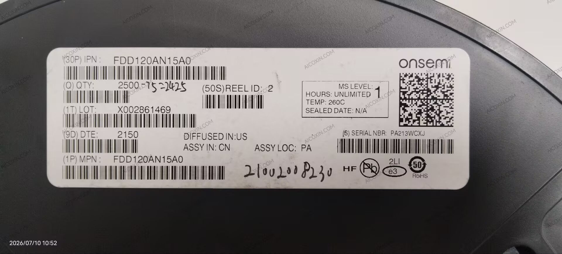
The onsemi FDD120AN15A0 is a 150V N-channel PowerTrench® MOSFET designed for efficient power switching and conversion. It supports a maximum continuous drain current of 14A at TC = 25°C with VGS = 10V and is suitable for synchronous rectification, uninterruptible power supplies, micro solar inverters, LED TVs, and consumer power applications.
At VGS = 10V and ID = 4A, the device provides 101mΩ typical and 120mΩ maximum RDS(on). At VGS = 6V and ID = 2A, maximum RDS(on) is 170mΩ. Gate threshold voltage is specified from 2V to 4V, with a maximum gate-to-source rating of ±20V.
The FDD120AN15A0 features a typical total gate charge of 11.2nC, 2.6nC typical Miller charge, and 770pF typical input capacitance. Its low Miller charge, low-Qrr body diode, and single-pulse and repetitive-pulse UIS capability make it well suited to switching power designs.
Maximum power dissipation is 65W, single-pulse avalanche energy is 122mJ, and the operating/storage junction temperature range is -55°C to +175°C. The device is supplied in a DPAK-3 / TO-252-3 package, with 2,500 devices per tape-and-reel. onsemi currently lists the part as Active, Pb-free, halide-free, and RoHS compliant.
Key Features:
- Manufacturer: onsemi
- Part Number: FDD120AN15A0
- Device Type: Power MOSFET
- Channel: N-Channel
- Technology: PowerTrench®
- Configuration: Single
- Drain-Source Voltage: 150V
- Maximum Drain Current: 14A at TC = 25°C
- Maximum RDS(on): 120mΩ at 10V
- Typical RDS(on): 101mΩ at 10V
- Gate Threshold Voltage: 2V to 4V
- Maximum Gate Voltage: ±20V
- Typical Total Gate Charge: 11.2nC
- Maximum Total Gate Charge: 14.5nC
- Typical Miller Charge: 2.6nC
- Typical Input Capacitance: 770pF
- Typical Output Capacitance: 85pF
- Single-Pulse Avalanche Energy: 122mJ
- Maximum Power Dissipation: 65W
- Junction Temperature Range: -55°C to +175°C
- Package: DPAK-3 / TO-252-3
- Packaging: Tape & Reel
- Reel Quantity: 2,500 pcs
- MSL: Level 1
- Pb-Free / Halide-Free / RoHS Compliant
- Product Status: Active.



Reviews
There are no reviews yet.