
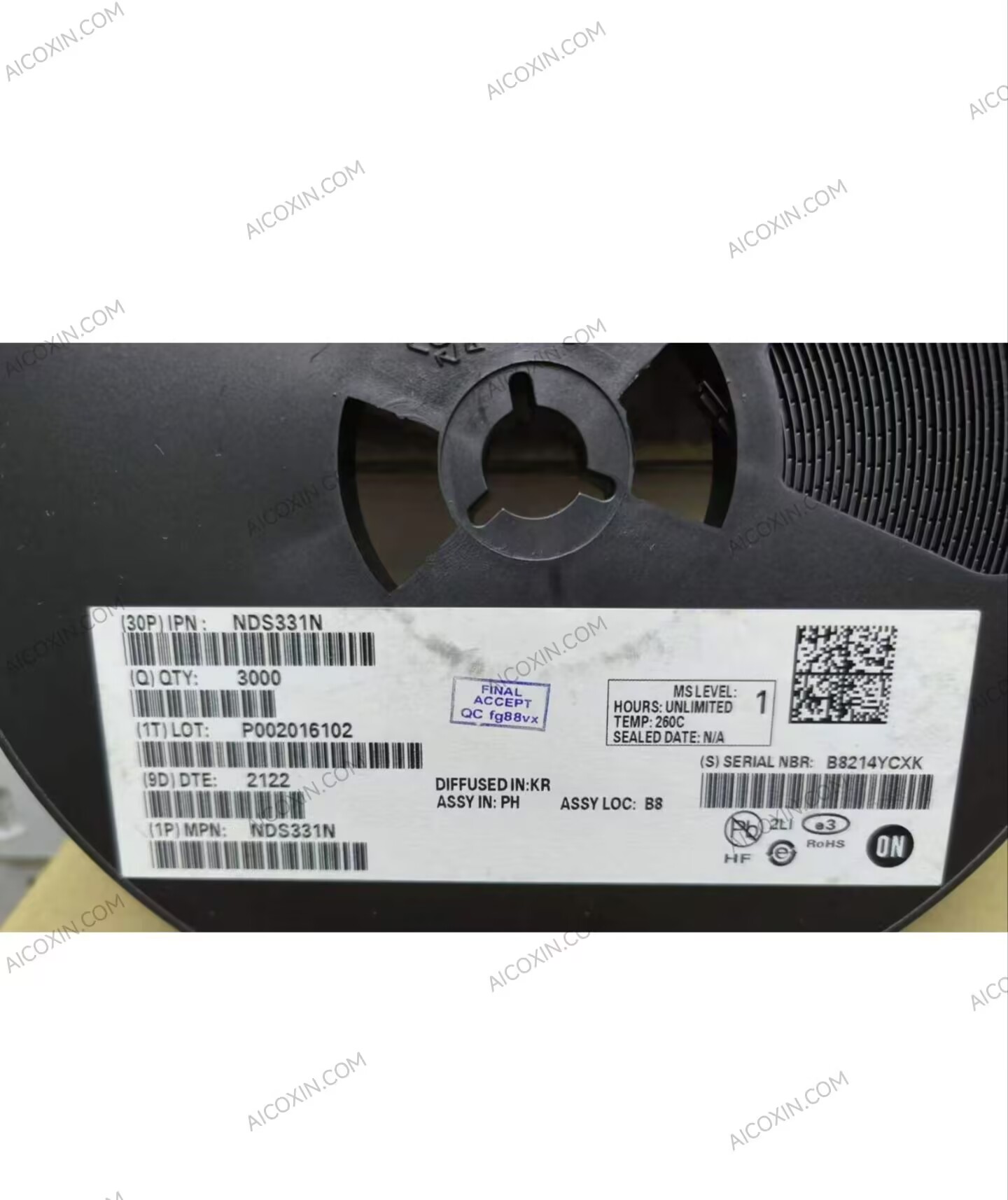


The onsemi NDS331N is a high-performance N-channel logic-level enhancement-mode MOSFET designed for efficient low-voltage switching, power management, and battery-powered electronic applications. Featuring a drain-source voltage rating of 20V and a continuous drain current rating of 1.3A at 25°C ambient temperature under specified PCB conditions, this transistor provides reliable switching performance in a compact SOT-23/SUPERSOT-23 surface-mount package.
Manufactured using onsemi’s proprietary high-cell-density DMOS technology, the NDS331N delivers low on-state resistance and excellent switching characteristics. It features a maximum drain-source on-resistance of 0.16Ω at VGS = 4.5V and ID = 1.5A, and 0.21Ω at VGS = 2.7V and ID = 1.3A. These characteristics make it suitable for low-voltage switching applications requiring reduced conduction losses and logic-level gate drive.
The device features a gate threshold voltage range of 0.5V to 1.0V, a typical total gate charge of 3.5nC, and a typical input capacitance of 162pF. Its low gate charge and fast switching capability support efficient operation in compact power management and electronic control circuits.
The NDS331N supports a maximum continuous gate-source voltage rating of ±8V and a maximum power dissipation of 0.5W under specified mounting conditions at 25°C. Its operating junction temperature range of -55°C to +150°C provides flexibility for various electronic environments.
Housed in an industry-standard SOT-23 package with onsemi’s SUPERSOT-3 design, the NDS331N offers compact dimensions and improved thermal and electrical performance. Its lead-free construction and tape-and-reel packaging support automated SMT assembly and high-density PCB applications.
Key Specifications:
- Manufacturer: onsemi (ON Semiconductor)
- Part Number: NDS331N
- Product Type: N-Channel Logic Level MOSFET
- Channel Configuration: Single N-Channel
- Operating Mode: Enhancement Mode
- MOSFET Technology: High-Density DMOS
- Drain-Source Voltage (VDS): 20V
- Continuous Drain Current (ID): 1.3A (TA = 25°C, Specified PCB Conditions)
- Pulsed Drain Current: 10A
- Maximum RDS(on): 0.16Ω (VGS = 4.5V, ID = 1.5A)
- Maximum RDS(on): 0.21Ω (VGS = 2.7V, ID = 1.3A)
- Gate Threshold Voltage (VGS(th)): 0.5V to 1.0V
- Typical Gate Threshold Voltage: 0.7V
- Maximum Gate-Source Voltage: ±8V
- Typical Total Gate Charge (Qg): 3.5nC
- Maximum Total Gate Charge: 5nC (Specified Test Conditions)
- Typical Input Capacitance (Ciss): 162pF
- Typical Output Capacitance (Coss): 85pF
- Typical Reverse Transfer Capacitance (Crss): 28pF
- Maximum Power Dissipation: 0.5W (Specified PCB Conditions, TA = 25°C)
- Typical Junction-to-Ambient Thermal Resistance: 250°C/W
- Operating Junction Temperature: -55°C to +150°C
- Package: SOT-23-3 / SUPERSOT-23
- Package Dimensions: Approximately 2.9 × 1.4mm
- Mounting Type: Surface Mount (SMD/SMT)
- Compliance: Pb-Free
- Packaging: Tape & Reel
- Standard Reel Quantity: 3,000 Pieces
Typical Applications:
- Low-voltage electronic switching
- Battery-powered electronic devices
- Portable computers and communication equipment
- Power management and load switching
- Mobile phones and handheld devices
- Microcontroller-controlled switching circuits
- Compact DC power control systems
- General-purpose electronic control circuits


Reviews
There are no reviews yet.