
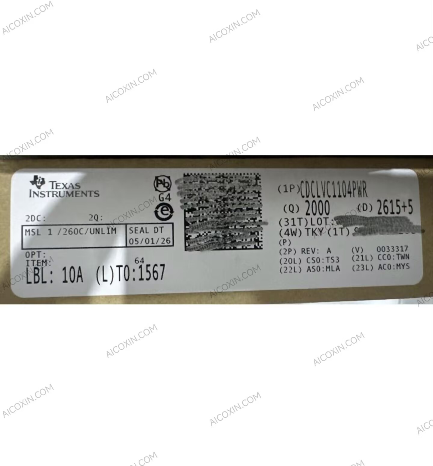
The Texas Instruments CDCLVC1104PWR is a high-performance, low-jitter 1:4 LVCMOS clock fanout buffer designed for accurate clock distribution in communication, industrial, and digital electronic systems. Featuring one LVCMOS clock input and four LVCMOS clock outputs, this device provides reliable clock signal distribution with low output skew and minimal additive jitter in a compact TSSOP-8 surface-mount package.
Part of TI’s CDCLVC11xx high-performance clock buffer family, the CDCLVC1104PWR supports clock frequencies up to 250MHz at a 3.3V supply voltage and 180MHz at a 2.5V supply voltage. Its low-skew architecture provides a maximum output-to-output skew of 50ps under equal loading conditions, helping maintain precise timing relationships between multiple clock destinations.
The device features a typical additive RMS jitter of 70fs, supporting low-noise clock distribution in timing-sensitive digital circuits. At a 3.3V supply, it offers a maximum propagation delay of 2.0ns and a maximum output rise/fall time of 0.8ns under specified test conditions.
The CDCLVC1104PWR includes an asynchronous output enable input (1G), allowing all four clock outputs to be enabled or disabled simultaneously. When the enable input is driven low, the outputs are forced to a low logic state, providing convenient clock distribution control and system-level power management functionality.
Supporting nominal 2.5V and 3.3V operation, the device is suitable for a variety of LVCMOS-based digital systems. Its operating temperature range of -40°C to +85°C supports applications in industrial control equipment, communication infrastructure, embedded computing, and general-purpose electronic systems.
Housed in an 8-pin TSSOP package, the CDCLVC1104PWR offers compact dimensions, RoHS-compliant construction, and tape-and-reel packaging, making it suitable for high-density PCB layouts and automated SMT assembly.
Key Specifications:
- Manufacturer: Texas Instruments (TI)
- Part Number: CDCLVC1104PWR
- Product Series: CDCLVC11xx
- Product Type: Clock Fanout Buffer IC
- Buffer Configuration: 1:4
- Number of Clock Inputs: 1
- Number of Clock Outputs: 4
- Input Signal Type: LVCMOS
- Output Signal Type: LVCMOS
- Maximum Clock Frequency: 250MHz (3.3V Supply)
- Maximum Clock Frequency: 180MHz (2.5V Supply)
- Nominal Supply Voltage: 2.5V / 3.3V
- Recommended Supply Range: 2.3V–2.7V or 3.0V–3.6V
- Typical Additive RMS Jitter: 70fs
- Maximum Output-to-Output Skew: 50ps
- Maximum Propagation Delay: 2.0ns (3.3V)
- Maximum Rise/Fall Time: 0.8ns (3.3V)
- Output Control: Asynchronous Output Enable (1G)
- Output State When Disabled: Logic Low
- Operating Temperature: -40°C to +85°C
- Package: TSSOP-8 (PW)
- Number of Pins: 8
- Package Body Dimensions: 3.0 × 4.4mm (Nominal)
- Mounting Type: Surface Mount (SMD/SMT)
- Moisture Sensitivity Level: MSL 1
- Compliance: RoHS and REACH Compliant
- Packaging: Tape & Reel
- Standard Reel Quantity: 2,000 Pieces
- Product Status: Active
Typical Applications:
- Clock distribution and fanout circuits
- High-speed digital communication systems
- Industrial automation and control equipment
- FPGA and microcontroller clock distribution
- Embedded computing platforms
- Digital signal processing systems
- Networking and communication equipment
- Consumer electronic devices
- Multi-device clock synchronization
- General-purpose PCB timing circuits


Reviews
There are no reviews yet.